In our quest to explore the mysteries of space, it is crucial to consider the environmental impact of our space missions. The European Space Agency (ESA) recognizes this responsibility and has embarked on a mission to assess and minimise the environmental footprint of its space endeavours. Through the Clean Space Initiative, ESA has actively engaged in Life Cycle Assessment (LCA) activities since 2012. In 2020, the Agency launched an Invitation to Tender to conduct an LCA of Green Electronics for Space. Electronics have been identified as a major environmental concern in ESA’s missions.
Contract Award
The contract for this study was awarded to a consortium led by imec, comprising OHB and VITO.
Understanding LCA at ESA
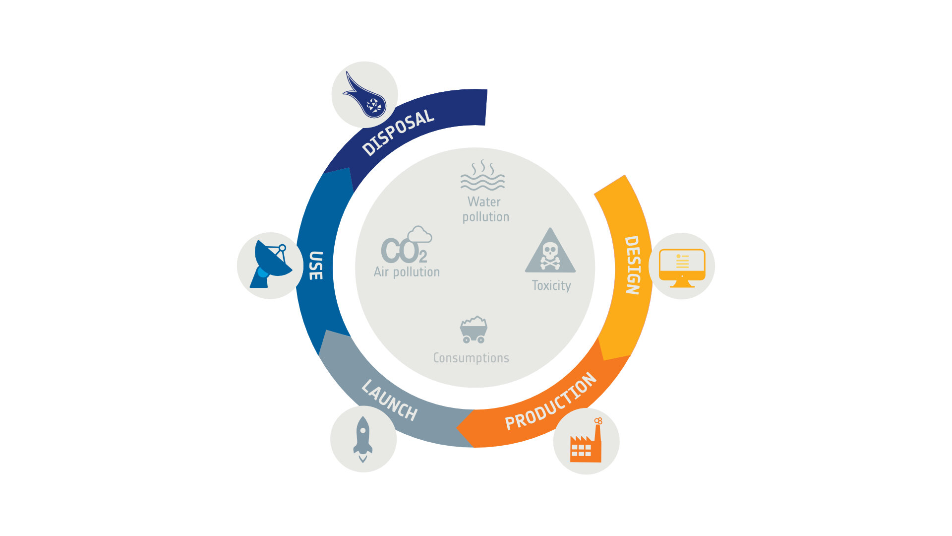
LCA serves as the backbone of ESA’s environmental assessment methodology. It is an ISO-standardized approach used to quantitatively assess the environmental impact of products and/or services. Widely accepted across industries and regulatory domains, LCA provides crucial insights into the environmental implications of our actions. ESA leverages LCA to assess the environmental impacts of spacecraft and launchers, focusing on environmental impact categories such as Global Warming Potential, Ozone Depletion Potential, and Human Toxicity Potential, among others. In fact, at ESA, more than 15 environmental impact categories are analysed through LCA.
Addressing the Environmental Hotspot: Electronics
Previous studies conducted by ESA have revealed that electronics play a significant role as an environmental hotspot in space missions. To tackle this issue, ESA is actively exploring alternative manufacturing processes, including the utilization of printed electronics. By optimizing the manufacturing and testing of electronics, we cannot only reduce their environmental impact but also enhance overall efficiency.
Objectives of the Invitation to Tender
The objective of the Invitation to Tender was to perform an LCA at different levels of spacecraft electronics, identify the most impactful aspects, evaluate alternative materials and processes, select environmentally friendly options, and develop a roadmap to increase the adoption of green electronics.
Eco-Design Measures: Making a Positive Impact
After a long and complex process with many experts and parties involved, the contractor has identified six eco-design measures that can be implemented without major impacts on manufacturing or product performance. These measures include eliminating certain processes, standardizing the use of specific materials, and transitioning to lead-free soldering which is today the industry standard. Imec and VITO assessed the environmental impact of implementing these measures and found positive results in most categories.
- Eliminate Degolding/Tinning of Terminals:
The current practice of covering electronic component terminals with thick gold for storage purposes results in a large consumption of gold – a metal with a huge environmental impact – without having any functional or performance value, and a large amount of gold contaminated solder waste when it needs to be removed before board assembly. By eliminating this process, we can reduce gold usage and solder waste while aligning space electronics with practices followed by the non-space industry.
- Industry Grade Terminal Solderability Requirements:
Requiring components with solderability properties according to J-STD-002 standards supports the previous measure, ensuring compatibility and promoting efficient assembly processes.
- Eliminate reflowed SnPb Finish Requirement:
The use of a reflowed SnPb finish on PCBs provides an efficient and eco-friendly solution in space electronics. However, it restricts interconnection density on PCB surfaces and relies on an outdated PCB manufacturing process no longer used by any other industry. Eliminating this finish requirement can reduce lead (Pb) usage, eliminate Pb-containing waste streams, phase-out the outdated reflow process and enable the use of solder mask. However, alternative finishes should be assessed for their environmental impact.
- Standardize the Use of Solder Mask:
Currently, complications during board assembly prevent the use of solder mask in combination with the SnPb solder finish. However, by utilizing alternative finishes, we can apply solder mask to protect non-soldered copper surfaces. This enables the creation of PCBs with higher track density, facilitating smaller and lighter electronics. It also allows for machine soldering of small pitch through-hole components and the use of advanced footprints.
- Lead-Free Soldering:
Lead-free soldering has become the standard in electronics assembly as a result of the RoHS-directive ban of lead in electronic and electrical equipment . Although it requires higher soldering energy and increased consumption of materials like tin (Sn) and silver (Ag) that have a larger negative environmental impact than Pb, it leads to a reduction in lead (Pb) usage and, especially, aligns space electronics with non-space industry practices eliminating the need for SnPb soldering compatible low volume processes and components.
- Standardize the Use of Plastic IC Packages:
Space electronics currently mandate hermetically packed IC components in metal or ceramic bodies, requiring high-temperature firing of ceramic substrates (LTCC @850-900oC, HTCC @1600oC). Allowing non-hermetic plastic packages would eliminate this energy-intensive process, resulting in significant energy savings. It would also lead to smaller, lighter components and better alignment with the non-space industry, where plastic packaging is commonly used.
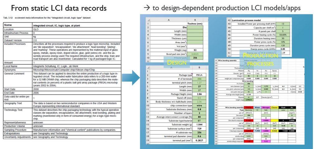
Parametric Life Cycle Inventory
Manufactured electronic elements (IC-dies, PCB, ceramic capacitors, film resistors…) may contain a wide variety of materials and vary orders of magnitude in size and weight, even if they represent similar functionality. The same is true for assembled electronic elements (Packaged ICs, Printed Board Assemblies…). Accurate Life Cycle Inventory (LCI) for electronics cannot be based on an “average” LCI dataset for a system element type that is merely scaled by weight, area, etc. LCI must be based on system element design and its manufacturing and assembly processes. During the activity, a novel parametric approach to LCI was developed and demonstrated for IC packaging, PCB manufacturing and component assembly.
Evaluation and Future Studies
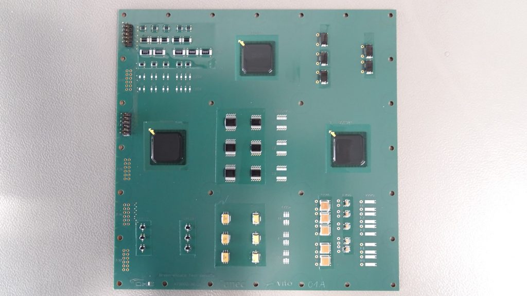
During the evaluation of ecodesign options using the PBA test vehicle, some interesting findings emerged. Although no failures occurred during electrical monitoring, cracks were discovered in the solder joints of all ceramic components when using the SAC305 solder alloy. On the other hand, the Innolot alloy performed well in testing, but further refinement of the reflow process is required to minimize voiding. The failures observed during testing have become the focus of ongoing and future studies on lead-free soldering for space applications. It is evident that the transition to more widely employed assembly processes is inevitable. This shift holds the promise of reducing the environmental impact of PCB assemblies for space applications in the long run.
Conclusion
The valuable insights gained from these tests and studies are crucial for improving the reliability and sustainability of space electronics. By addressing the challenges encountered and optimizing assembly techniques, we can pave the way for greener and more resilient electronic systems in space.
The journey toward reducing environmental impact continues, driven by ongoing research and the determination to advance the future of space technology. Furthermore, it is recommended to enhance LCA models and data collection for PCB manufacturing, IC-packaging, and assembly while expanding the LCA approach to include cabling and mechanics. Emphasizing the need to adapt industry standards to facilitate eco-design options is also essential.
Together, we can make space exploration a sustainable and eco-friendly endeavour.


Discussion: no comments